
IR905 Datasheet
Features
- •GaAlAs double heterostructure technology
- •Peak wavelength: 905 nm (IF = 20 mA)
- •Optical power: 1–2.2 mW (IF = 20 mA)
- •Low forward voltage: 1.2–1.6 V (IF = 20 mA)
- •Customizable chip size — contact sales
- •Gold metallization: top ≥ 14000 Å, bottom ≥ 8000 Å
- •Chip thickness: 254 ± 50 µm (10 ± 2 mils)
- •N cathode top contact, P anode bottom contact
- •ESD sensitive — handle with proper precautions
- •RoHS compliant
Typical Applications
- •LiDAR & time-of-flight (ToF) sensors
- •Automotive ADAS & autonomous driving
- •3D depth sensing & mapping
- •Drone & UAV obstacle detection
- •Industrial distance measurement
- •Robotics navigation & collision avoidance
- •Surveying & topographic mapping
- •Security perimeter detection
Die Outline & Delineation


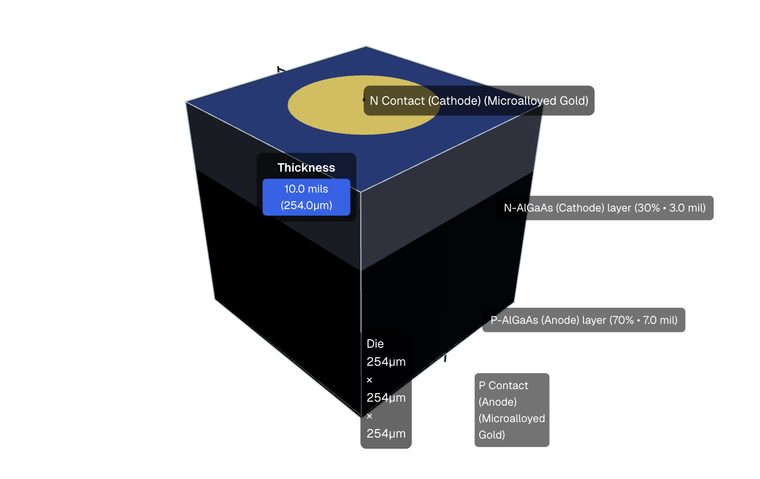
Mechanical Parameters
| Parameter | Minimum | Typical | Maximum | Unit |
|---|---|---|---|---|
| Chip Size | — | Customizable | — | µm |
| Chip Thickness | 204 | 254 | 304 | µm |
| Chip Thickness | 8 | 10 | 12 | mils |
| Top Contact | N Cathode (AuGe metallization ≥ 14000 Å) | — | ||
| Bottom Contact | P Anode (AuZn metallization ≥ 8000 Å) | — | ||
| Top Metallization (Au) | 14000 | — | — | Å |
| Bottom Metallization (Au) | 8000 | — | — | Å |
Absolute Maximum Ratings (TA = 25°C unless otherwise noted)
Stresses beyond these values may permanently damage the device. Functional operation outside of these limits is not implied.
| Parameter | Symbol | Rating | Unit |
|---|---|---|---|
| DC Forward Current (continuous) | IF | 80 | mA |
| Pulse Forward Current (tp = 100 µs, D = 0) | IFP | 1000 | mA |
| Reverse Voltage (IR = 10 µA) | VR | 5 | V |
| Operating Temperature Range | TOP | −40 to +85 | °C |
| Junction Temperature | TJ | 125 | °C |
| Storage Temperature | TSTG | 15 to 30 | °C |
Electro-Optical Characteristics (TA = 25°C)
| Parameter | Symbol | Test Condition | Min | Typ | Max | Unit |
|---|---|---|---|---|---|---|
| Static Characteristics | ||||||
| Peak Wavelength | λpeak | IF = 20 mA | — | 905 | — | nm |
| Spectral Half-Width (FWHM) | Δλ | IF = 20 mA | — | 50 | — | nm |
| Optical Power Output | Po | IF = 20 mA | 1.0 | — | 2.2 | mW |
| Forward Voltage | VF | IF = 20 mA | 1.2 | — | 1.6 | V |
| Reverse Voltage | VR | IR = 10 µA | 5 | — | — | V |
¹ Typical values represent median of distribution. Min/Max represent guaranteed limits tested at production. Measurements performed with an accuracy of ±15%. Contact sales@manuled.com for application-specific characterization.
Handling, Storage & Ordering
ESD Sensitivity: Devices are ESD-sensitive. Handle with proper grounding straps and ESD-safe workstations.
Storage: Store wafers in sealed, dry nitrogen environment at 15–30°C and relative humidity < 60%. Vertical storage recommended.
Shelf Life: Storage time is not limited by the die itself when kept in original hermetically sealed packaging.
Packaging: Bare die supplied on ring frame. Lot traceability maintained.
Pricing: Starting from $0.10 (< 1M units) · Starting from $0.07 (≥ 1M units). Volume pricing and custom configurations available.
DISCLAIMER: MANULED provides the information in this document in good faith but assumes no liability arising from its use. Typical parameters may vary between applications and over time. All operating parameters, including typical values, must be validated for each customer application by the customer's technical experts. MANULED reserves the right to make changes to products or specifications at any time without notice. Products are not designed or authorized for use in life-support, military, or safety-critical applications without prior written consent. Product specifications do not expand MANULED's terms and conditions of sale. RoHS compliant. All values are at TA = 25°C unless otherwise stated. © 2026 MANULED. All rights reserved.
Typical Characteristic Curves (TA = 25°C unless noted)
Charts show typical characteristics. Actual values may vary. Contact sales@manuled.com for measured data.